- 您现在的位置:买卖IC网 > Sheet目录1992 > DAC5674IPHPG4 (Texas Instruments)IC DAC 14BIT 400MSPS 48-HTQFP
DAC5674
SLWS148A SEPTEMBER 2003 REVISED OCTOBER 2005
www.ti.com
19
080
IF=32
160
240
320
112
208
0
100
IF=40
200
300
400
260
140
065
IF=26
130
195
260
91
169
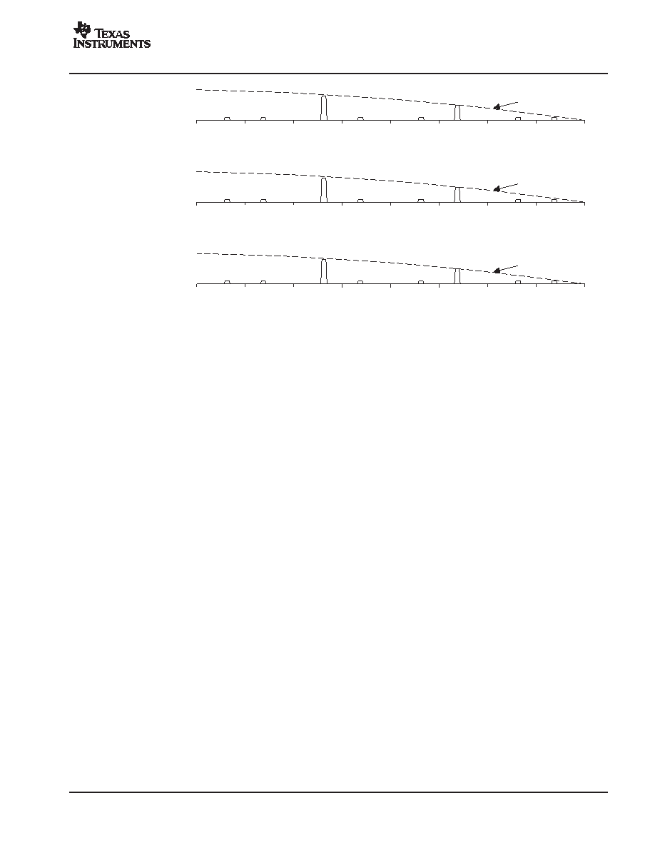
”Sinx/x”
Attenuation
Fupdate+65 MSPS
*1.83 dB
*7.2 dB
”Sinx/x”
Attenuation
Fupdate+80 MSPS
*1.83 dB
*7.2 dB
”Sinx/x”
Attenuation
Fupdate+100 MSPS
*1.83 dB
*7.2 dB
Figure 20. High-Pass 4
y Interpolation Filter Operation: Example Frequencies
Clock Generation Function
An internal phase-locked loop (PLL) or external clock can be used to derive the internal clocks (1
×, 2×, and 4×)
for the logic, FIR interpolation filters, and DAC. Basic functionality is depicted in Figure 21. Power for the internal
PLL blocks (PLLVDD and PLLGND) is separate from the other clock generation blocks power (CLKVDD and
CLKGND), thus minimizing phase noise within the PLL. The PLLVDD pin establishes internal/external clock
mode: when PLLVDD is grounded, external clock mode is active and when PLLVDD is 3.3 V, internal clock mode
is active.
In external clock mode, the user provides a differential external clock on pins CLK/CLKC. This clock becomes
the 4
× clock and is twice divided down to generate the 2× and 1× clocks. The 2× or 1× clock is multiplexed out
on the PLLLOCK pin to allow for external clock synchronization.
In internal clock mode, the user provides a differential external reference clock on CLK/CLKC. A type four
phase-frequency detector (PFD) in the internal PLL compares this reference clock to a feedback clock and
drives the PLL to maintain synchronization between the two clocks. The feedback clock is generated by dividing
the VCO output by 1
×, 2×, 4×, or 8×, as selected by the prescaler (DIV[1:0]). The output of the prescaler is the
4
× clock, and is divided down twice to generate the 2× and 1× clocks. Pin X4 selects the 1× or 2× clock to clock
in the input data; the selected clock is also fed back to the PFD for synchronization. The PLLLOCK pin is an
output indicating when the PLL has achieved lock. An external RC low-pass PLL filter is provided by the user
at pin LPF. See the Low-Pass Filter section for filter setting calculations. Table 4 provides a summary of the
clock configurations with corresponding data rate ranges.
发布紧急采购,3分钟左右您将得到回复。
相关PDF资料
DAC7621EBG4
IC SNGL 12BIT PARALLEL D/A 20SSO
DAC7801KPG4
IC DUAL 12BIT CMOS DAC 24-DIP
DAC8043AESZ
IC DAC 12BIT MULT SRL INP 8SOIC
DAC8043GP
IC DAC 12BIT MULTIPLY CMOS 8-DIP
DAC8221GP
IC DAC 12BIT DUAL W/BUFF 24-DIP
DAC8222GPZ
IC DAC 12BIT DUAL W/BUFF 24DIP
DAC8229FSZ-REEL
IC DAC 8BIT DUAL V-OUT 20SOIC
DAC8248FS
IC DAC 12BIT DUAL W/BUFF 24-SOIC
相关代理商/技术参数
DAC5674IPHP-ND
制造商: 功能描述: 制造商:undefined 功能描述:
DAC5674IPHPR
功能描述:数模转换器- DAC 14-Bit 400 CommsDAC RoHS:否 制造商:Texas Instruments 转换器数量:1 DAC 输出端数量:1 转换速率:2 MSPs 分辨率:16 bit 接口类型:QSPI, SPI, Serial (3-Wire, Microwire) 稳定时间:1 us 最大工作温度:+ 85 C 安装风格:SMD/SMT 封装 / 箱体:SOIC-14 封装:Tube
DAC5674IPHPRG4
功能描述:数模转换器- DAC 14-Bit 400 CommsDAC RoHS:否 制造商:Texas Instruments 转换器数量:1 DAC 输出端数量:1 转换速率:2 MSPs 分辨率:16 bit 接口类型:QSPI, SPI, Serial (3-Wire, Microwire) 稳定时间:1 us 最大工作温度:+ 85 C 安装风格:SMD/SMT 封装 / 箱体:SOIC-14 封装:Tube
DAC5675
制造商:TI 制造商全称:Texas Instruments 功能描述:14-BIT, 400-MSPS DIGITAL-TO-ANALOG CONVERTER
DAC5675A
制造商:TI 制造商全称:Texas Instruments 功能描述:14-Bit, 400MSPS Digital-to-Analog Converter
DAC5675AEVM
功能描述:数据转换 IC 开发工具 DAC5675A Eval Mod RoHS:否 制造商:Texas Instruments 产品:Demonstration Kits 类型:ADC 工具用于评估:ADS130E08 接口类型:SPI 工作电源电压:- 6 V to + 6 V
DAC5675AIPHP
功能描述:数模转换器- DAC 14-Bit 400-MSPS RoHS:否 制造商:Texas Instruments 转换器数量:1 DAC 输出端数量:1 转换速率:2 MSPs 分辨率:16 bit 接口类型:QSPI, SPI, Serial (3-Wire, Microwire) 稳定时间:1 us 最大工作温度:+ 85 C 安装风格:SMD/SMT 封装 / 箱体:SOIC-14 封装:Tube
DAC5675AIPHP
制造商:Texas Instruments 功能描述:IC DAC 14BIT 400MSPS 48-HTQFP